Contact:Mr Wang
Mobile :13713335011
Wechat:13713335011
Fax:0769-89783666
Tel :0769-89783666
Email:wym@oikwan.com.cn
Add :5th Floor, Building D, No. 19 Zhugang Road, Shatou, Chang'an Town, Dongguan City

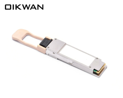
40Gb/s QSFP+ Active Optical Cable
Product Features
1.Full duplex 4 channel 850nm parallel active optical cable
2.Up to 11.1Gbps Data rate per channel
3.Maximum link length of 300m links on OM3 multimode fiber
4.High Reliability 850nm VCSEL technology
5.Electrically hot-pluggable
6.Case operating temperature range: 0°C to 70°C
7.Power dissipation < 1.5 W per cable end
Applications
40G Ethernet
Infiniband QDR
Fiber channel
HPC Interconnections
Standard
Compliant to QSFP+ MSA
RoHS Compliant
Product selection
Part Number | Product description |
QSFP+-AOC-XXX | XXX=different cable lengths on OM3 Multimode Fiber (MMF) –Note |
XXX | cable lengths on OM3 Multimode Fiber (MMF)-max 300m |
003 | 3m |
005 | 5m |
007 | 7m |
010 | 10m |
050 | 50m |
100 | 100m |
Note:
More detail product selection and cable lengths,please contact sales。
Ⅰ Absolute Maximum Ratings
Parameter | Symbol | Min. | Typ. | Max. | Unit | Note |
Storage Temperature | Ts | -40 | - | 85 | ºC | |
Relative Humidity | RH | 5 | - | 95 | % | |
Power Supply Voltage | VCC | -0.3 | - | 4 | V | |
Signal Input Voltage | Vcc-0.3 | - | Vcc+0.3 | V |
Ⅱ Recommended Operating Conditions
Parameter | Symbol | Min. | Typ. | Max. | Unit | Note |
Case Operating Temperature | Tcase | 0 | - | 70 | ºC | Without air flow |
Power Supply Voltage | VCC | 3.14 | 3.3 | 3.46 | V | |
Power Supply Current | ICC | - | 450 | mA | per cable end | |
Data Rate | BR | 10.3125 | Gbps | Each channel |
Ⅲ General Product Characteristics
Parameter | Value | Unit | Notes |
Module Form Factor | QSFP+ | ||
Number of Lanes | 4 Tx /Rx | ||
Maximum Aggregate Data Rate | 42.0 | Gb/s | |
Maximum Data Rate per Lane | 10.5 | Gb/s | |
Standard Cable Lengths | 3, 5, 7, 10, 50, 100 | meters | Other lengths, please contact sales |
Protocols Supported | Typical applications include Infiniband, Fiber Channel, 40G Ethernet | ||
Electrical Interface and Pin-out | 38-pin edge connector | Pin-out as defined by the QSFP+ MSA | |
Standard Optical Cable Type | Multimode ribbon fiber cable assembly, riser-rated | ||
Maximum Power Consumption per End | 1.5 | W | |
Management Interface | Serial, I2C-based, 400 kHz maximum frequency | As defined by the QSFP+ MSA |
IV. Electrical Characteristics
Parameter | Symbol | Min | Typ | Max | Unit | NOTE |
Supply Voltage | Vcc1,VccTx,VccRx | 3.14 | 3.3 | 3.46 | V | |
Supply Current | Icc | 450 | mA | |||
Transmitter | ||||||
Differential data input swing | Vin,pp | 180 | 1000 | mV | 1 | |
Single ended input voltage tolerance
| VinT
| -0.3
| 4.0
| V | ||
Receiver | ||||||
Vout,pp | 300 | 850 | mV | 2 | ||
Single-ended output voltage
| -0.3
| 4.0
| V |
Notes:
1. AC coupled internally. See Figure 1 for input eye mask requirements. Self-biasing 100Ω differential input.
2. AC coupled with 100Ω differential output impedance. See Figure 2 for output eye mask.
![]()
Figure 1 – Transmitter Input Differential Signal Mask
![]()
Figure 2 – Receiver Output Differential Signal Mask
V. High-speed Electrical Characteristics per Lane
Parameter-Inputs | Symbol | Min | Typ | Max | Unit | NOTE |
Reference Differential Input Impedance | Zd
| 100 | Ω
| |||
Termination Mismatch | ΔZM
| 5 | %
| 1 | ||
Input AC Common Mode Voltage | 25 | mV (RMS) | ||||
Differential Input Return Loss
| SDD11
| dB | 2 ,0.01-4.1 GHz | |||
dB | 3,4.1 – 11.1 GHz
| |||||
Differential to Common Mode Loss
| SCD11 | -10 | dB | 0.01-11.1 GHz
| ||
Jitter Tolerance (Total) | TJ | 0.40 | UI | |||
Jitter Tolerance (Deterministic) | DJ | 0.15 | UI |
Notes:
1. See SFF-8431 section D.15 Termination Mismatch for definition & test recommendations
2. Reflection coefficient given by equation SDD11(dB)< -12+2*SQRT(f), with f in GHz. See Figure 3.
3. Reflection coefficient given by equation SDD11(dB)< -6.3+13Log10(f/5.5), with f in GHz. See Figure 3
![]()
Figure 3 – Maximum Transmitter Input and Receiver Output Differential Return Loss
Parameter-Outputs | Symbol | Min | Typ | Max | Unit | NOTE |
Reference Differential Output Impedance | Zd
| 100 | Ω
| |||
Termination Mismatch | ΔZM
| 5 | %
| |||
Output AC Common Mode Voltage | 15 | mV (RMS) | ||||
Differential Output Return Loss
| SDD22
| dB | 4 ,0.01-4.1 GHz | |||
dB | 5 ,4.1 – 11.1 GHz | |||||
Common Mode Output Return Loss
| SCC22
| dB | 6,0.01-2.5 GHz | |||
-3 | dB | 2.5-11.1 GHz | ||||
Output Rise and Fall time (20% to 80%) | tRH, tFH
| 24 | ps | |||
Deterministic Jitter | DJOUT | 0.38 | UI | 7 | ||
Total Jitter | TJOUT | 0.64 | UI | 7 |
Notes:
4. Reflection coefficient given by equation SDD22(dB)< -12+2*SQRT(f), with f in GHz. See Figure 3.
5. Reflection coefficient given by equation SDD22(dB)< -6.3+13Log10(f/5.5), with f in GHz. See Figure 3.
6. Reflection coefficient given by equation SCC22(dB)< -7+1.6*f, with f in GHz.
7. When transmitter input jitter specs are met.
VI. Pin Assignment
![]()
Figure 4---Pin out of Connector Block on Host Board
Pin | Symbol | Name/Description | NOTE |
1 | GND | Transmitter Ground (Common with Receiver Ground) | 1 |
2 | Tx2n | Transmitter Inverted Data Input | |
3 | Tx2p | Transmitter Non-Inverted Data output | |
4 | GND | Transmitter Ground (Common with Receiver Ground) | 1 |
5 | Tx4n | Transmitter Inverted Data Input | |
6 | Tx4p | Transmitter Non-Inverted Data output | |
7 | GND | Transmitter Ground (Common with Receiver Ground) | 1 |
8 | ModSelL | Module Select | |
9 | ResetL | Module Reset | |
10 | VccRx | 3.3V Power Supply Receiver | 2 |
11 | SCL | 2-Wire serial Interface Clock | |
12 | SDA | 2-Wire serial Interface Data | |
13 | GND | Transmitter Ground (Common with Receiver Ground) | |
14 | Rx3p | Receiver Non-Inverted Data Output | |
15 | Rx3n | Receiver Inverted Data Output | |
16 | GND | Transmitter Ground (Common with Receiver Ground) | 1 |
17 | Rx1p | Receiver Non-Inverted Data Output | |
18 | Rx1n | Receiver Inverted Data Output | |
19 | GND | Transmitter Ground (Common with Receiver Ground) | 1 |
20 | GND | Transmitter Ground (Common with Receiver Ground) | 1 |
21 | Rx2n | Receiver Inverted Data Output | |
22 | Rx2p | Receiver Non-Inverted Data Output | |
23 | GND | Transmitter Ground (Common with Receiver Ground) | 1 |
24 | Rx4n | Receiver Inverted Data Output | 1 |
25 | Rx4p | Receiver Non-Inverted Data Output | |
26 | GND | Transmitter Ground (Common with Receiver Ground) | 1 |
27 | ModPrsl | Module Present | |
28 | IntL | Interrupt | |
29 | VccTx | 3.3V power supply transmitter | 2 |
30 | Vcc1 | 3.3V power supply | 2 |
31 | LPMode | Low Power Mode,not connect | |
32 | GND | Transmitter Ground (Common with Receiver Ground) | 1 |
33 | Tx3p | Transmitter Non-Inverted Data Input | |
34 | Tx3n | Transmitter Inverted Data Output | |
35 | GND | Transmitter Ground (Common with Receiver Ground) | 1 |
36 | Tx1p | Transmitter Non-Inverted Data Input | |
37 | Tx1n | Transmitter Inverted Data Output | |
38 | GND | Transmitter Ground (Common with Receiver Ground) | 1 |
Notes:
1. GND is the symbol for signal and supply (power) common for QSFP+ modules. All are common within the QSFP+ module and all module voltages are referenced to this potential unless otherwise noted. Connect these directly to the host board signal common ground plane.
2. VccRx, Vcc1 and VccTx are the receiving and transmission power suppliers and shall be applied concurrently. Recommended host board power supply filtering is shown below. Vcc Rx, Vcc1 and Vcc Tx may be internally connected within the QSFP+ transceiver module in any combination. The connector pins are each rated for a maximum current of 500mA.
VII. Host - Transceiver Interface Block Diagram
VIII. Outline Dimensions
![]()